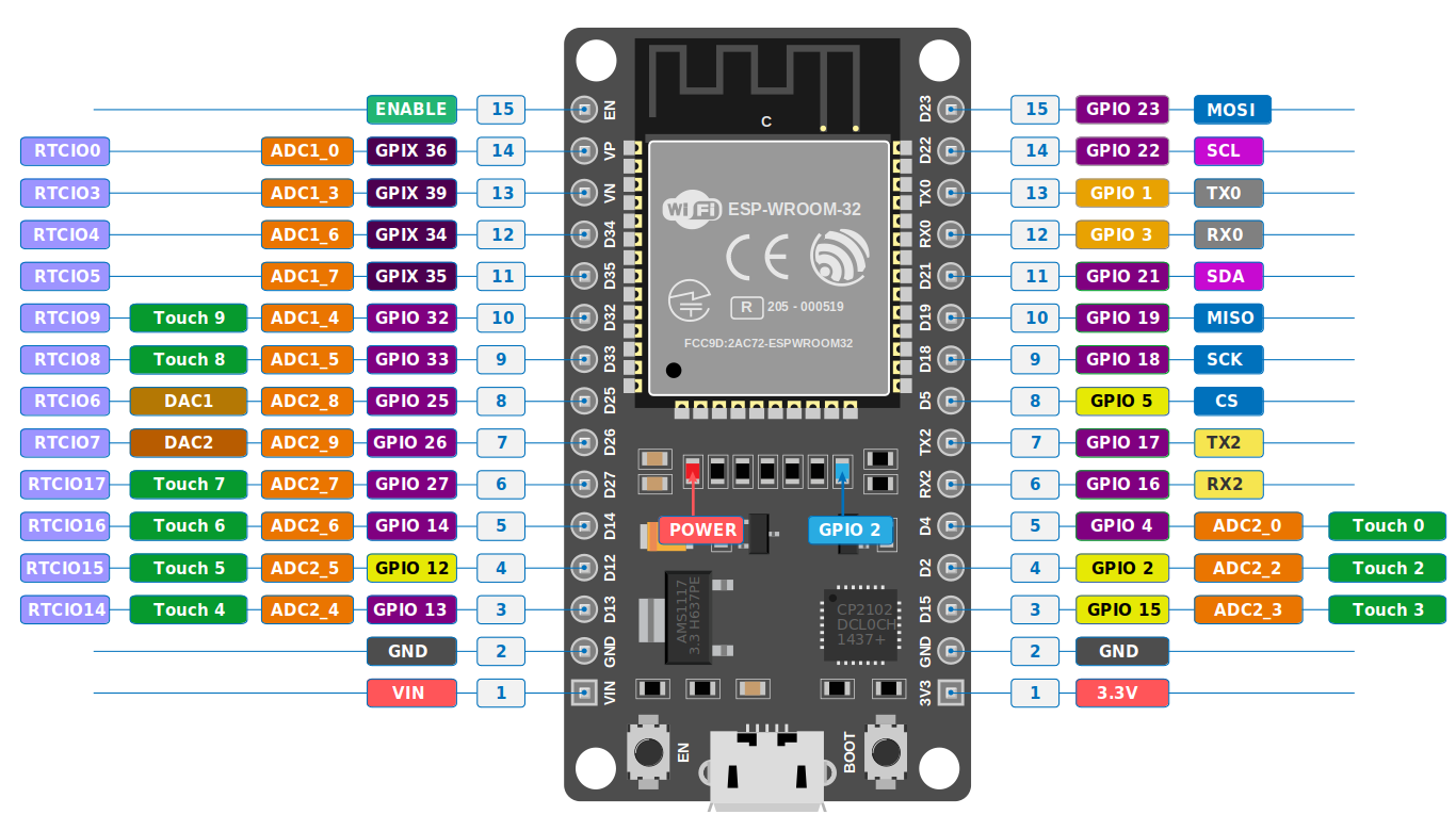
ESP32 Pinout
License: CC-BY-SA 4.0
The above pinout diagram is derivative from the original diagram created by the CircuitState website. They also have provided detailed explanations for each pin. You can check it out here.
Disclaimer: This book is not affiliated with nor associated with CircuitState. I am including this diagram as i found it helpful during my research.
Keypoints
-
Input-Only GPIOs: GPIO pins 34, 35, 36, and 39 are input-only and cannot be used as output pins. In the pinout diagram, these pins are labeled with a "GPIX" prefix and marked with an "X" to indicate output is not allowed. Whenever possible, prefer using the pins highlighted in purple on the diagram.
-
Flashing and Debugging: GPIO 1 (Tx) and GPIO 3 (Rx) are designated for flashing and debugging purposes.
-
ADC Pins: Pins labeled as
ADC1_[Number]are associated with ADC1, while those labeled asADC2_[Number]are associated with ADC2.
